In this short introduction you will discover why photonic chips are attracting attention across UK data centres, AI centres and communications networks. Photonic chips are integrated circuits that use photons — particles of light — instead of electrons to send data and, increasingly, to perform computation. This shift underpins a new class of photonic processors and optical chips that promise distinct optical computing advantages for specific workloads.
Compared with silicon CPUs, photonics vs silicon discussions often focus on measurable benefits: far higher bandwidth over distance, lower latency for long links, improved energy efficiency in certain tasks, and better thermal characteristics in dense racks. These strengths make light-based computing a natural partner for fibre networks and many machine-learning pipelines.
Industry momentum is clear. Intel, IBM, Hewlett Packard Enterprise, Cisco and startups such as Lightmatter and PsiQuantum are investing heavily, while academic hubs like the University of Cambridge, the University of Oxford and MIT continue to drive core research. In this article you will first learn the fundamentals of how photonic devices operate, then examine componentry and fabrication, compare performance against traditional silicon CPUs, explore practical application areas, and finish with the integration challenges and likely future trajectory.
The tone is practical and aimed at readers in the United Kingdom who need to assess whether photonic processors and optical chips belong in their infrastructure roadmaps. Throughout, the focus will be on clear, second-person guidance so you can judge the real-world merits of light-based computing for your projects.
What are photonic chips and how they work
You will find photonic chips use light rather than moving electrons to carry information. This change shifts key limits on speed and energy use. Understanding what are photonic chips helps you see why companies such as Intel and Cisco invest in silicon photonics for data-centre interconnects.
At a basic level, optical computation encodes data onto light using amplitude, phase, polarisation and wavelength. That encoded light travels through on‑chip pathways and performs routing, switching and linear operations without the resistive losses common in electronic wiring.
The following sections break down the fundamentals and the parts you will meet when you inspect a photonic circuit.
Fundamentals of light-based computation
Photons move at the speed of light in the chip medium and avoid many thermal losses that plague electrons. You can encode information in multiple degrees of freedom, which gives optical computation high signalling flexibility.
Photonic circuits can carry out analogue operations natively. Non‑linear optics and electro‑optical conversion let you implement logic‑like functions or specialised analogue compute tasks. Distinguish between optical interconnects, which shuttle data between modules, and fully integrated photonic processors that aim to compute on‑chip.
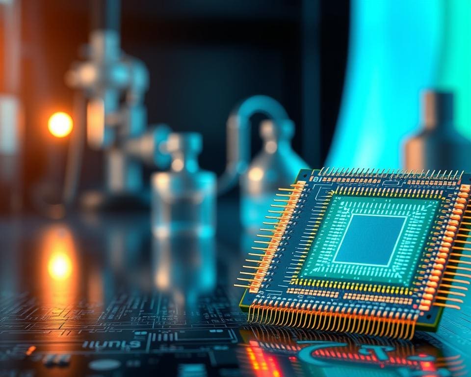
Key components: waveguides, modulators and detectors
Waveguides form the optical highways on a chip. Materials such as silicon and silicon nitride confine light in single‑mode or multi‑mode geometries. You will see bends, splitters and directional couplers for routing and interfacing with fibres.
Modulators convert electrical signals into changes in light. Common examples include Mach–Zehnder interferometers and carrier‑depletion modulators in silicon. These devices work at GHz to tens of GHz rates for data encoding.
Detectors perform the reverse task by turning light back into electrical signals. On‑chip germanium photodiodes are widespread in silicon photonics. You will also encounter PIN and avalanche photodiodes when higher responsivity or sensitivity is needed.
Other photonic components include micro‑ring resonators for wavelength selection, optical amplifiers when gain is required, switches, couplers for fibre interfaces and grating couplers for efficient fibre‑to‑chip links.
Materials and fabrication methods for photonic devices
Silicon photonics builds on CMOS‑compatible processes and links to foundries such as TSMC, GlobalFoundries and IMEC research initiatives. That compatibility makes co‑integration with electronics viable and supports volume manufacturing.
Silicon nitride is chosen for very low loss across wide wavelength ranges. III–V semiconductors such as indium phosphide and gallium arsenide supply on‑chip lasers and optical gain, often added through heterogeneous integration or hybrid bonding to silicon platforms.
Fabrication uses advanced lithography, including DUV and EUV, plus plasma etching, wafer bonding and flip‑chip assembly for photonic–electronic integration. Packaging remains a critical challenge: fibre coupling, thermal control and sub‑micrometre alignment drive cost and yield issues in integrated photonics fabrication.
You will find active development in industry and academia. Work at Cambridge’s Cavendish Laboratory and Oxford University pushes device concepts, while firms such as Lightmatter explore photonic accelerators for AI. These efforts aim to improve component performance and scale up manufacturing routes for practical deployment.
Performance advantages of photonic chips over silicon CPUs
You will notice lower signal delay when light replaces electrons for many links. Photons travel with minimal degradation in waveguides and fibres, so optical vs electronic latency falls most when distances grow from on‑chip traces to board and rack spans.
Optical links already reach 100 Gbps and 400 Gbps per wavelength in commercial products. Research demonstrations combine many wavelengths to form aggregate Tbps channels, cutting end‑to‑end latency by removing repeated electrical regeneration.
Latency and bandwidth: how light speeds data transfer
In contexts such as high‑frequency trading, telecoms and HPC, shaving microseconds or even nanoseconds can matter. You get that advantage because propagation delay on photonic paths beats comparable copper runs, while device ecosystems scale to multi‑hundred‑Gbps lanes.
Parallelism and wavelength-division multiplexing for higher throughput
Wavelength-division multiplexing lets many wavelength channels carry different streams down one waveguide. That multiplies throughput without adding physical conductors, which suits dense datacentre fabrics.
Photonic parallelism goes beyond wavelengths. Chips can use spatial and modal channels, optical switching and reconfigurable meshes to run massive concurrent flows. Optical matrix ops perform linear algebra tasks in parallel, useful for machine learning workloads that strain electronic ALUs.
Thermal behaviour and energy efficiency compared with electronic processors
Electronic interconnects generate resistive heat that rises with switching and clock rates. As you pack more transistors into CPUs, cooling becomes a larger cost and design constraint in servers and blades.
Photonics avoids resistive heating along the signal path and often shows better photonic energy efficiency for long, high‑bandwidth links. Silicon‑photonic links commonly consume less energy per bit than copper beyond centimetre to metre scales, so you can reduce power in rack‑level and centre‑scale networks.
Be aware that modulators, drivers, detectors and optical–electrical conversion add overhead. Off‑chip lasers and thermal tuning of resonant devices also draw power, so net gains are highest where photonics replaces long, power‑hungry electrical interconnects or when optical computing cuts the number of electronic operations.
- Lower propagation delay improves optical vs electronic latency across system tiers.
- Wavelength-division multiplexing multiplies usable bandwidth without extra traces.
- Photonic parallelism enables concurrent processing and high aggregate throughput.
- Photonic energy efficiency is strongest for long distances and specialised optical primitives.
Practical applications where photonic chips excel
Photonic chips applications are moving from labs into real deployments. You can spot them in core networking gear and experimental compute nodes. These chips change how you design systems by shifting bandwidth, latency and power profiles.
In a photonic data centre you gain denser, lower-power links between racks and across sites. Vendors such as Cisco, Juniper and Arista already integrate photonic modules into switches and routers. You will see fewer copper cables, simpler topologies and lower cooling demands when optical transceivers replace traditional links.
Photonic switching fabrics let you reallocate capacity on the fly. That reduces congestion for cloud storage and high-throughput services. Operators meet sustainability and density goals while improving throughput for latency-sensitive workloads.
For machine learning, a photonic AI accelerator can speed up dense matrix maths. Companies like Lightmatter and Microsoft research projects have shown prototypes that target inference for large transformer models. You keep electronic control and memory, but offload heavy linear algebra to optical matrix units when throughput and power efficiency matter.
Hybrid photonic–electronic designs are the near-term route to production. You benefit from lower latency and high parallelism for specific layers of neural networks. This makes photonic AI accelerator approaches attractive for inference at scale.
Optical sensing suits photonic chips by nature. You can integrate light sources, filters and detectors on a single die for compact LIDAR, biosensing and spectrometry modules. That gives you smaller, more sensitive devices for medical diagnostics and environmental monitoring.
Communications and edge photonics converge in 5G/6G fronthaul and metro links. Photonic chips enable radio-over-fibre and high-bandwidth backhaul with reduced power use. At the network edge you lower round-trip times and avoid sending raw data to distant centres when real-time action is needed.
Edge photonics also supports autonomous vehicles and industrial automation. On-device inference and local optical interconnects cut data transfer to central systems. You get faster decisions for safety-critical tasks and reduced connectivity costs.
- Data centres and high-performance networking: optical interconnects, reduced cabling and reconfigurable networks.
- Artificial intelligence acceleration: analogue photonic matrix units for inference and hybrid architectures.
- Sensing and communications: compact optical sensing, radio-over-fibre and edge photonics for real-time use.
Major cloud providers and telecom operators run pilots and trials with silicon photonics. You will find proof-of-concept photonic accelerators in research centres and early-stage deployments for niche workloads. These pilots demonstrate where photonic chips applications yield tangible gains for scale and latency-critical systems.
Challenges, integration and the future of photonic chips
You will face several technical and manufacturing hurdles when evaluating photonic chips. Precision packaging and fibre coupling demand tighter tolerances than typical silicon chips, and thermal tuning of resonant devices adds design complexity and power overhead. These photonic chips challenges also include heterogeneous steps such as bonding III–V lasers and integrating germanium detectors, which raise process complexity and yield risks.
Integrating photonics and electronics remains central to practical deployment. Expect hybrid architectures where optics handle high-bandwidth and latency‑sensitive paths while CMOS controls logic and memory. The software side must evolve too: new toolchains and photonic design kits will be essential to turn lab gains into production value. Foundries such as GlobalFoundries and Intel, and consortia in the UK, are improving design flows and test infrastructure but gaps persist.
Economic and system-level factors will guide adoption. Upfront capital for fab upgrades and photonic manufacturing can be high, so assess vendor roadmaps, packaging strategies and ecosystem support before you commit. In the near term (2–5 years) expect wider use in data‑centre interconnects and niche AI accelerators; medium term (5–10 years) should bring better on‑chip lasers and mature PDKs, while long term (10+ years) could enable broader photonic chip scaling and hybrid co‑processors.
From a UK perspective, investment in the future of photonics supports semiconductor resilience and net‑zero targets if lifecycle impacts are managed. If you design for telecoms, data centres or edge AI, review hybrid options now and prioritise suppliers who demonstrate scalable manufacturing, robust packaging and software ecosystems to make photonics a practical, long‑term choice.